English
 Español
 tiếng việt
 русский
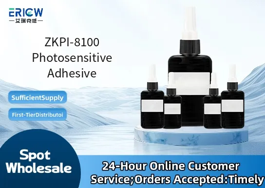
High-resolution patterning capability with sub-25 µm line/space definition under standard UV exposure (i-line, 365 nm).
Excellent thermal stability up to 220 °C for post-exposure curing and subsequent processing steps.
Low outgassing profile suitable for vacuum-based microfabrication environments (e.g., MEMS, display backplanes).
Chemically resistant to common developers (0.26 N TMAH) and mild etchants (dilute HCl, buffered HF).
Reproducible adhesion performance on silicon, glass, stainless steel, and ITO-coated substrates.
Temporary bonding/debonding in silicon-through-glass (TGV) and fan-out wafer-level packaging (FOWLP).
Photo-defined adhesive layers for flexible printed circuit (FPC) interposer assembly.
Patterning of dielectric spacers in micro-LED transfer printing processes.
UV-curable masking layer in precision metal etching for RF filter components.
Adhesive integration in hybrid bonding stacks for advanced image sensors.
| Chemical Type | Positive-tone phenolic novolac resin with diazonaphthoquinone (DNQ) photosensitizer |
| Product Form | Ready-to-use liquid solution (solvent-based) |
| Appearance | Clear, amber-colored viscous liquid |
| Viscosity (25 °C) | 18–22 cP (Brookfield LVDV-II+ with spindle #18) |
| Primary Applications | Temporary bonding, photo-definable adhesive, precision masking |
| Key Features | UV-sensitive, thermally stable, low ionic contamination |
| Benefits | High process yield, minimal residue after debonding, compatibility with cleanroom Class 100 |
| Regulatory Compliance | REACH SVHC compliant; RoHS 2015/863 Annex II compliant; no intentional PFAS |
| Common Compatible Systems | Suitability |
| Canon FPA-3030 i-Line Stepper | Highly Recommended – Optimized exposure dose: 120–160 mJ/cm² |
| Screen Printing & UV Curing Line (e.g., Dainippon Screen MEE) | Recommended – Requires pre-bake at 90 °C/90 sec and post-exposure bake at 110 °C/60 sec |
| Automated Wafer Bonding Tools (e.g., EVG® 850LT) | Highly Recommended – Validated for 200 mm / 300 mm temporary bonding cycles |
| TMAH-Based Spray Developer Systems (e.g., Tokyo Electron ACT 8) | Suitable – Standard 0.26 N concentration; development time: 45–60 sec at 23 °C |
Q1: What is the CAS Registry Number for ZKPI-8100?
A: The CAS number for ZKPI-8100 Photosensitive Adhesive (as supplied) is 2257432-88-9. Note that this refers to the formulated product; individual components are listed separately in the Safety Data Sheet (SDS).
Q2: What is the recommended coating thickness and corresponding spin speed for 6-inch wafers?
A: For a target dry-film thickness of 8–12 µm, spin coat at 2500 rpm for 30 seconds using a standard semiconductor coater. Thickness uniformity is typically ±3% across the wafer.
Q3: How does ZKPI-8100 compare to conventional non-photosensitive temporary adhesives like BCB or polyimide-based films?
A: Unlike non-photosensitive alternatives, ZKPI-8100 enables direct lithographic patterning without lamination or etch-back steps—reducing process complexity, material waste, and defect density. It also offers faster debonding kinetics at lower temperatures (≤180 °C) versus thermally cured BCB (>250 °C).
Q4: Is ZKPI-8100 compliant with food-contact or medical device regulations?
A: ZKPI-8100 is not intended for food-contact or implantable medical applications. It is designed exclusively for industrial microfabrication. No FDA 510(k), ISO 10993, or EU Food Contact Material (EC 10/2011) certifications apply.
Q5: Has migration or extractables testing been performed under typical processing conditions?
A: Yes. GC-MS and ICP-MS analysis per SEMI F57-0218 confirmed <1 ppm total organic extractables and <0.1 ppb metallic ions (Na, K, Fe, Cu) after full process flow (coat–prebake–expose–postbake–develop–rinse–dry) on silicon wafers.
Contact With Us:
E-mail: wangxingqiang@ericwchem.com
Have a Questions? Call Us:
Add:
Building A1, Jiete Industrial Park, Huangpu District, Guangzhou City, Guangdong Province, China