English
 Español
 tiếng việt
 русский
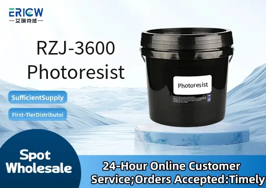
High-resolution patterning capability with sub-micron resolution down to 0.8 µm using standard i-line (365 nm) exposure tools.
Excellent thermal stability up to 130 °C, enabling robust post-exposure bake (PEB) and etch resistance in semiconductor and MEMS fabrication.
Low outgassing profile under vacuum conditions, minimizing contamination in lithography steppers and EUV pre-chamber environments.
Optimized adhesion to silicon, SiO₂, SiNₓ, and metal substrates (Al, Cu, TiW) without mandatory HMDS priming.
Environmentally enhanced formulation with reduced aromatic solvent content and compliant with VOC emission guidelines (EPA Method 24).
Semiconductor front-end-of-line (FEOL) gate and contact layer patterning for 0.13–0.25 µm CMOS processes.
MEMS device fabrication including accelerometers, gyroscopes, and microfluidic channel definition.
Power device manufacturing (IGBTs, SiC diodes) requiring thick-film (>3 µm), high-etch-selectivity resist layers.
Advanced packaging applications such as redistribution layer (RDL) and fan-out wafer-level packaging (FOWLP).
Flat-panel display (FPD) array substrate patterning for TFT-LCD and AMOLED backplanes.
| Chemical Type | Novolac resin-based positive photoresist with diazonaphthoquinone (DNQ) photosensitizer |
| Product Form | Liquid concentrate (ready-to-use), supplied in 1-gallon HDPE carboys and 4-liter stainless steel cans |
| Appearance | Clear, pale yellow to amber viscous liquid; free of gels and particulates |
| Viscosity (25 °C) | 22–26 cP (measured per ASTM D445) |
| Primary Applications | i-line (365 nm) photolithography for semiconductor, MEMS, and advanced packaging |
| Key Features | High sensitivity (~40–60 mJ/cm²), wide process latitude, low standing wave effect |
| Benefits | Reduced defect density, improved CD uniformity (<±3% 3σ), compatibility with aqueous TMAH developers |
| Regulatory Compliance | REACH SVHC-free; RoHS 2015/863 compliant; no intentionally added PFAS or PFOA |
| Common Compatible Systems | Suitability |
| ASML PAS 5500 / i-line steppers | Highly Recommended – Validated for full-field exposure with <±1.5% dose uniformity |
| Tokyo Electron (TEL) CLEAN TRACK ACT series (ACT-12, ACT-8) | Highly Recommended – Fully integrated process recipes available (coating, PEB, develop) |
| Screen SemiCoat SC-1000 spin coater | Recommended – Requires minor nozzle calibration; film thickness CV <2.5% |
| Dainippon Screen (DNS) SD series developers | Suitable – Compatible with 0.26 N TMAH; developer temperature control ±0.3 °C critical |
| Karlsuss MA6 mask aligner | Suitable – Achieves >90% line fidelity at 2 µm features; contact mode only |
Q1: What is the CAS Registry Number for RZJ-3600 Photoresist?
A: RZJ-3600 is a proprietary multi-component formulation; individual CAS numbers are assigned to key constituents (e.g., novolac resin: 9003-35-4; DNQ: 86-73-7). Full compositional disclosure requires signed CDA.
Q2: What is the typical coating thickness and recommended spin speed range for 3.0 µm target film?
A: For 3.0 µm nominal thickness on bare silicon wafers, use 2500–2800 rpm for 30 seconds (acceleration 500 rpm/sec); final thickness tolerance: ±0.15 µm (3σ) under controlled temp/humidity (22±1°C, 45±5% RH).
Q3: How does RZJ-3600 compare to GBL-1200 in terms of resolution and etch resistance?
A: RZJ-3600 offers superior resolution (0.8 µm vs. 1.2 µm for GBL-1200) and ~25% higher etch resistance in CF₄/O₂ plasma, but requires tighter PEB temperature control (±0.5°C vs. ±1.5°C for GBL-1200).
Q4: Is RZJ-3600 certified for use in medical device manufacturing per ISO 10993 or USP Class VI?
A: RZJ-3600 is not intended for direct patient-contact applications. It meets ISO 14644-1 Class 5 cleanroom handling standards and has passed extractables testing per USP <661.1>, but full ISO 10993 biocompatibility assessment requires end-device level validation.
Q5: Are there known migration or leaching concerns when RZJ-3600 residues remain after stripping in copper interconnect processes?
A: Residual carbonized resist is effectively removed by standard sulfuric acid/peroxide (SPM) or oxygen plasma ashing. Trace metal analysis (ICP-MS) shows Cu, Al, and Fe leaching <0.05 ppb post-strip—well below SEMI F57 limits for 300 mm wafer fabs.
Contact With Us:
E-mail: wangxingqiang@ericwchem.com
Have a Questions? Call Us:
Add:
Building A1, Jiete Industrial Park, Huangpu District, Guangzhou City, Guangdong Province, China